Circuits Board (Computers - Hardware)

Item ID 2621955 in Category: Computers - Hardware
Circuits Board | |
The Circuits Board layer that has a sizable region loaded up with conductive material is known as a copper pour. Copper pours can be utilized to increment warm execution and proposition an incredibly low-obstruction or low-inductance association between parts. A plane layer is a PCB layer that is made totally of a solitary, significant copper pour. We normally place vias nearby part pins to make ground associations and go about as a ground plane on an interior layer. Contact Info:- High Quality PCB Co., Limited Office: Shajing Town, Baoan District, Shenzhen, Guangdong 518000, China Plant 1 address: Building 5-6, Fu Qiao 3rd Industrial Zone, Bao' an, Shenzhen, Guangdong, China Plant 2 address: Zhuhai, Guangdong, China Plant 3 address: Dongguan, Guangdong, China TEL: +86-755-23724206 WahtsApp: +86-189 2381 2997 Skype: shawnwang2006 Email: sales@efpcb.com 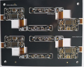 | |
| Related Link: Click here to visit item owner's website (0 hit) | |
| Target State: All States Target City : Shenzhen Last Update : 01 July 2023 8:41 PM Number of Views: 108 | Item Owner : Shawn Wang Contact Email: Contact Phone: +86-755-23724206 |
| Friendly reminder: Click here to read some tips. | |
© 2024 INNetAds.com
USNetAds.com | GetJob.us | CANetAds.com | UKAdsList.com | AUNetAds.com | CNNetAds.com | Hot-Web-Ads.com | USAOnlineClassifieds.com
2024-04-30 (0.388 sec)